Time:2023-09-08 Read:326
Since the 2000s, with the development of nanotechnology, various nanomaterials with a feature size in the range of 1-300 nm have been used in a wide range of areas. Significant efforts have been devoted to studying the strong light-matter interactions at the nanoscale. Noble metal nanomaterials such as gold, silver, and copper have attracted considerable interest because of their special properties like catalytic activity, fluorescence characteristics, and surface plasmon (SP). Therein, the SPs are extremely sensitive to properties of the nanoparticles and the surrounding medium, resulting in their good performance as sensors. For extended metal surfaces, this gives rise to surface plasmon polaritons (SPPs), a state of evanescent wave, which are localized on the surface of metal by the interaction of electrons and photons, and surface plasmon waves (SPW) propagating at the metal-dielectric interface. For metal nanoparticles, the response arises from localized surface plasmons (LSPs), whose resonances depend on the particle material, size, and shape. When a metal nanoparticle surrounded by a dielectric is excited by electromagnetic radiation, its free electrons will oscillate collectively through resonant interaction with the incident electromagnetic field. This process is called localized surface plasmon resonance (LSPR) and shows broad potential for application in nanophotonic, materials science, life science, and environmental engineering. Based on the control of surface plasmon wave (SPW) of nanoparticles, many practical applications have been reported, such as surface-enhanced Raman scattering (SERM), display technology, medical diagnosis and therapy, biosensing and bioimaging, solar cells, micro/nano devices, and so on.
Moreover, one of the most important properties of SP is its capability to overcome the classical diffraction limit and manipulate light at the subwavelength scale. A feature of surface plasmons is that they are localized at much smaller scales than the wavelength of incident light, which is of significant interest to the developments in highly-integrated photonics, and in data storage applications. Thus, localizing or confining light in a smaller area is critical to numerous fields, including integrated photonics, subwavelength optics, optical data storage, super-resolution microscopy techniques such as tip-based near-field scanning microscopy (SNOM), and lithography. However, the large losses due to the oscillatory absorption of free electrons and small transmission distance make it difficult to achieve a strong local field enhancement and perfect transmission feature without high transmission loss, which limits further application. Moreover, the cumbersome and sophisticated mechanical systems required for manipulating the tip of tip-based SNOM to probe the sample of interest severely restricts the potential for miniaturization. Additionally, the sample must be pre-treated and fixed for analysis with tip-based SNOM, causing difficulties with implementing real-time detection of changes in the sample.
In this work, we have developed gold nanostructures with nanodisk, cuboidal and triangular geometries that enable the focusing and guiding of surface plasmon waves (SPW) Moreover, the sample of interest can be transported to the focusing region by microchannel without the cumbersome mechanical manipulation system, permitting real-time analysis. Through numerical simulations and experiments with TM/TE polarization, we have demonstrated that SPWs can be transported between different nanostructures with the bulk of SPW power being focused at the tip of the nanostructure. Notably, we have achieved perfect transmission features without loss due to eigenmode resonance, and have observed an order of magnitude enhancement in the power of the electromagnetic field at the focusing tip. The transfer distance and orientation of the focusing point can be tailored for specific applications. Furthermore, we have designed and implemented double nanostructures for enhanced light-matter interaction, which has been applied to the development of a sensor capable of detecting and distinguishing non-living and living components.
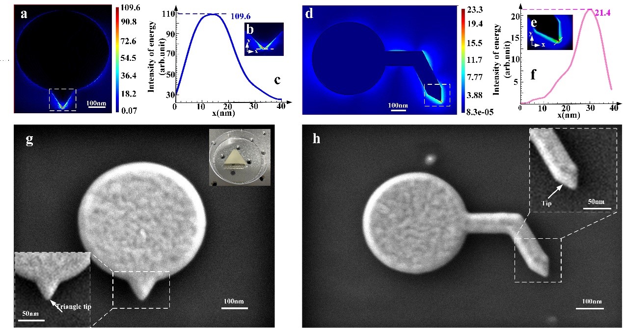
Figure. (a, d) Simulations of a 500 nanometer-sized gold nanodisk with a 50 nm gold triangle tip and a 50 nm zigzag with a gold triangle tipped rod, respectively. (b, e) Magnified figures of the area in the dotted box of Figure (a, d), respectively. (c, f) The energy intensity distributions on the transversal dotted line of graph (b, e), respectively. (g, h) The SEM image of the manufactured nanostructures, respectively. Scale bar, 100 nm.
The research was published in “Hongrui Shan, Hailang Dai, Qiheng Wei, and Xianfeng Chen, Focusing of Surface Plasmon Wave for Small-Molecule Sensing, Advanced Photonics Research, 2300165 (2023)”.
Link: https://onlinelibrary.wiley.com/doi/full/10.1002/adpr.202300165