Time:2021-12-21 Read:1886
Photolithography technology is one of the key drivers of our modern scientific and technological society. It has many applications in integrated circuit fabrication, microelectronics, and micro-nanofabrication. Therefore, to achieve a nanoscale lithography technology that can break through the limitations of existing technology is an irresistible target with the rapid development of science and technology. We know that the linewidth and etching depth of nanopatterns are significant indicators of photolithography technology, and the final aim of research in this field is to obtain a nanolithography technology that is cost-effective and produces a narrow linewidth.
In this letter, we present a method that allows sub-100-nm lines to be patterned photolithographically using ultrahigh-order modes from a symmetrical metal-cladding waveguide (SMCW) in the near field, which are excited by continuous wave visible light without focusing. The etching depth of the nanopattern reaches more than 200 nm. The localized light intensity distribution can be used to map the photoresist exposure pattern, which agrees well with our theoretical model. UOMs have a narrow linewidth and a high power density in the mode oscillating zone. Meanwhile, the effective refractive index of the SMCM is very small due to the small incident angle, which indicates that the group velocity of the UOMs is close to zero in the transmission direction. Hence, the coupled light is confined to a small zone, which causes coherent oscillation in the guiding layer, resulting in an enhancement of the oscillation field in the small coherent oscillation zone. The linewidth of the guided mode resonance with high energy density can reach the nanoscale, enabling the diffraction limit to be broken. Therefore, we have designed a system and an experimental setup to demonstrate the linewidth and etching depth of UOM nanoscale photolithography technology with experimental data. Meanwhile, the linewidth of photolithography can be controlled by adjusting the distance between the waveguide and the photoresist and by changing the thickness of the guiding layer. This technique opens up the possibility of localizing light fields below the diffraction limit using maskless and lower power visible light.
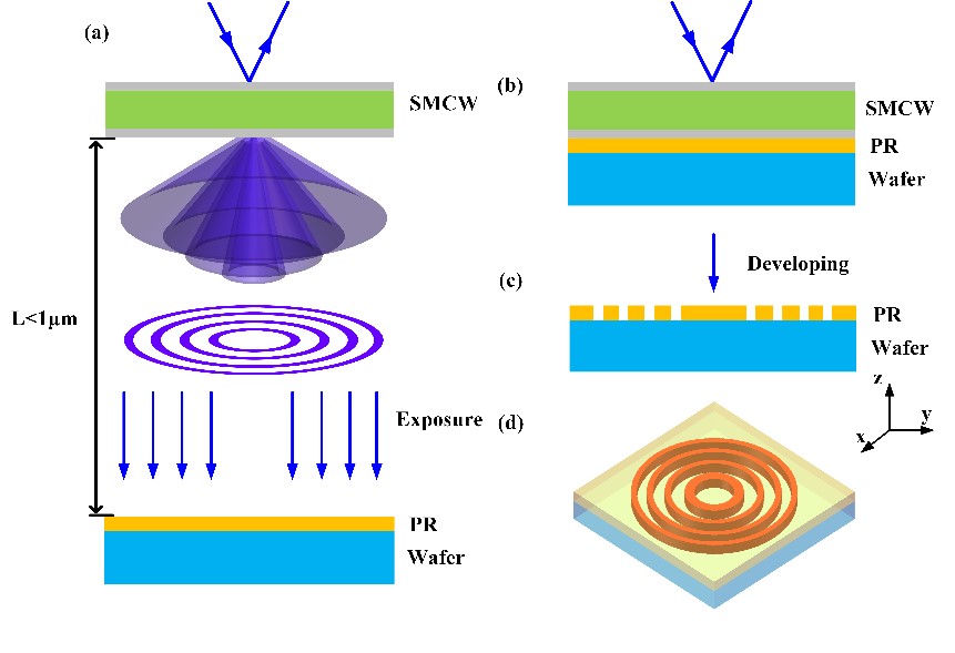
Fig. 1. Schematic of the UOM photolithography system. (a) Transmitted light cones formed by leakage radiation from the UOMs. (b) Photoresist (PR) is subjected to UOM exposure. (c) After exposure, the photoresist is developed. (d) Schematic of the photolithography pattern.
The research was published in “Meng Zhang, Hailang Dai,Yuxi Shang, Zhuangqi Cao, and Xianfeng Chen, Maskless nanostructure photolithography by ultrahigh-order modes of a symmetrical metal-cladding waveguide, Optics letters, 47, 62-65 (2022)”.
Link: https://doi.org/10.1364/OL.446431